A few days ago I posted my driver prototype for a 20 W, 700 mA, 32 V white LED. Under best conditions I reached 85% of power conversion efficiency between the 12 V input and the electrical power delivered to the LED. I was not satisfied and one of my suspicions were substantial losses in the power MOSFET.
I had copied drive circuit which boosts the output from the integrated switch-mode power supply driver from an application note which also had been used by other projects on the internet. After a bit of simulation and a bit of testing I was able to decrease the power losses by another watt, increasing the measured efficiency at an LED current of 700 mA from 83% to 86%.

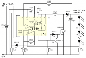
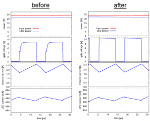
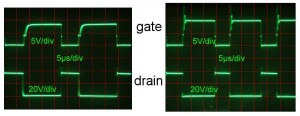
If you compare both circuits you will notice the absence of the 160 Ω resistor between the output of the 78S40 and the base of the PNP transistor Q1. A resistor here could prevent a bipolar transistor from going into saturation, however, Q1 is not actively driven from the chip! The output of the chip is an open emitter of an NPN transistor only capable of sourcing current, but not sinking it. The only thing this resistor does is to slow down the charging of the MOSFET’s gate and thus delaying the off-on transient of the MOSFET. Also the 1.6%nbsp;kΩ resistor between the gate and ground does not really make sense, since the gate is actively discharged through the PNP transistor in the absence of a positive drive signal from the 78S40. The resulting change in the simulated and measured wave forms can be seen in the following figures.


The off-on transient of the MOSFET has become much crisper, both in the simulations and in reality. And the real MOSFET now stays a lot cooler, while the inductor still gets warm – so that’s where the losses are…

