Here is a brief follow up from yesterday’s post on the internal reference voltage VBG of the ATmega328P.
I wrote a small test program where I wait for a variable delay time after switching the input multiplexer of the analog-to-digital converter to the internal bandgap reference voltage VBG. Using the AVcc of ![]() as the conversion reference I then calculate the apparent supply voltage assuming a known VBG of
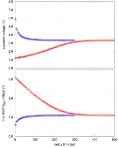
as the conversion reference I then calculate the apparent supply voltage assuming a known VBG of ![]() . The result can be seen in the upper half of the plot below. The lower half of the plot shows the actual input voltage to the ADC, this means the voltage available for conversion on the sample-and-hold capacitor.
. The result can be seen in the upper half of the plot below. The lower half of the plot shows the actual input voltage to the ADC, this means the voltage available for conversion on the sample-and-hold capacitor.

Timing behavior of the internal bandgap reference voltage VBG of an ATmega328P when connecting the VBG as an input to the ADC.
The blue curve corresponds to a switching between GND and VBG on the multiplexer. The low-resistive GND connection discharges the sample-and-hold capacitor of the analog-to-digital converter, which then is slowly charged up again from a highly-resistive VBG source. As a result the calculated supply voltage is assumed to be much higher than the actual voltage.
The red curve shows the behavior when the input of the ADC was connected to AVcc before switching the multiplexer to the VBG source. Here the sample-and-hold capacitor has to be discharged through the highly-resistive VBG source.
It is also apparent from the plots that the internal VBG connection to the multiplexer is much better in sourcing than sinking current. While the sourcing has the appearance of an exponential RC timing, the sinking looks more like a constant-current discharge with a fixed compliance voltage.
If the worst-case scenario cannot be excluded you should wait for
after switching the MUX to VBG before starting the analog-to-digital conversion in the ATmega328P.


[…] ATmega328P – measuring its own supply voltage II […]