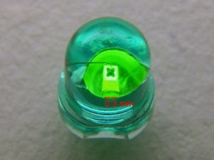
I have always been fascinated by knowing what’s inside electronics. And this does not stop by looking inside electronic apparatus — it continues into the packages of the individual electronic devices. Take the green light-emitting diode which I chose as this blog’s logo:
There is nothing special to this LED. It probably dates from the 1980’s or 1990’s and is not one of the popular modern super-bright versions. Inside the clear epoxy package you can see the tiny piece of semiconductor, a cube with edges about 0.3 mm in length.
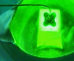
In the case of this LED this crystal is made of gallium phosphide. Constructed as a pn-junction diode green photons with an energy of 2.23 eV each are emitted when electrons and holes recombine. The crystal is mounted inside a tiny metal bowl which acts as a reflector and at the same time provides the electrical contact to the negative cathode at the bottom of the crystal. The contact to the positive anode at the top of the crystal is made with a tiny wire with an estimated diameter of 0.03 mm (corresponding to AWG46).
Perhaps another interesting detail is how I took these photos. I used my digital SLR, a Pentax K200D, a manual focus 50 mm prime lens and a set of two extension tubes with lengths of 12 mm and 36 mm. The LED was powered from a 3 V lithium cell, hidden underneath a sheet of paper. Because of the spherical shape of the LED package itself, the semiconductor crystal appears somewhat magnified


Very nice vidps3atxvipx
What youre saying is entirely accurate. I know that everybody need to say the same thing, but I just assume that you simply put it in a way that everyone can comprehend. I also love the images you place in here. They fit so nicely with what youre trying to say. Im confident youll reach a great number of people with what youve got to say.